Quantum devices
Here you can find pictures of processed devices and illustrations made by our lab. Please click on the pictures to enter the view mode!
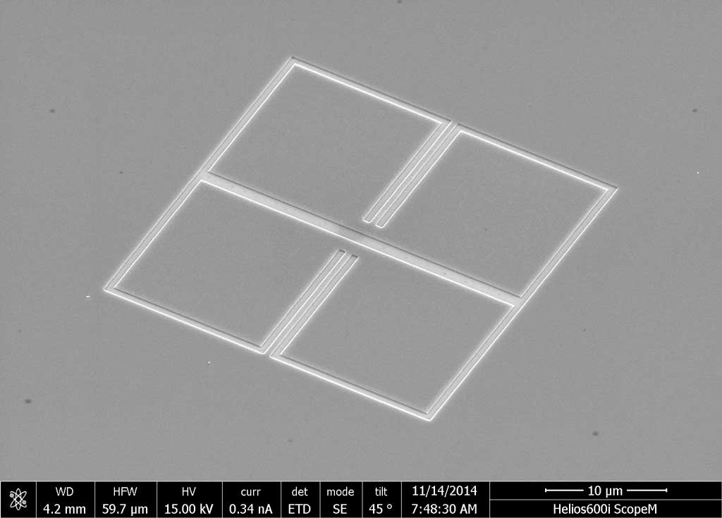
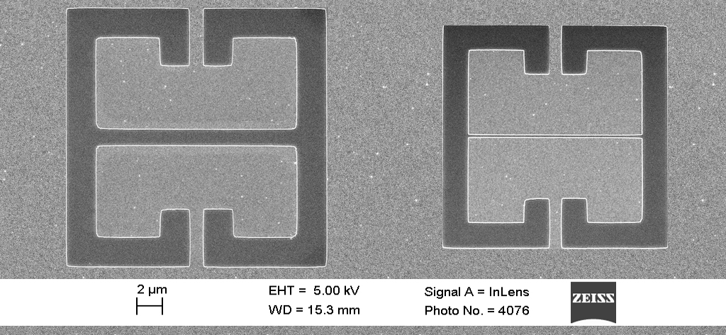
Electron microscope image of split-ring resonator
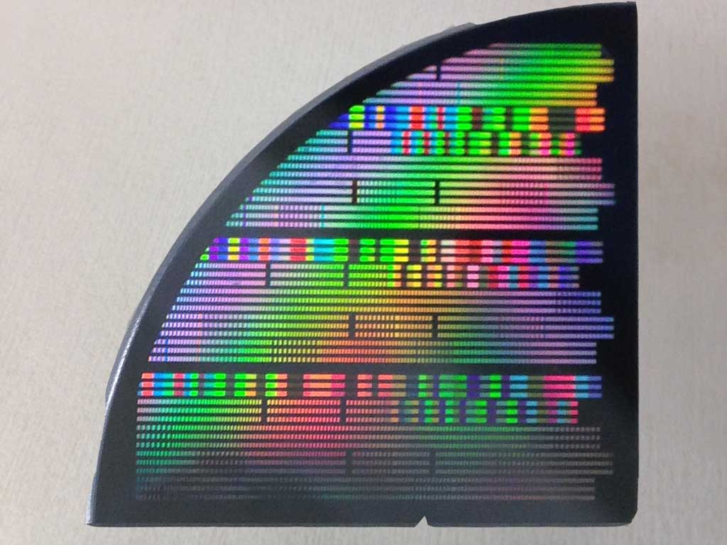
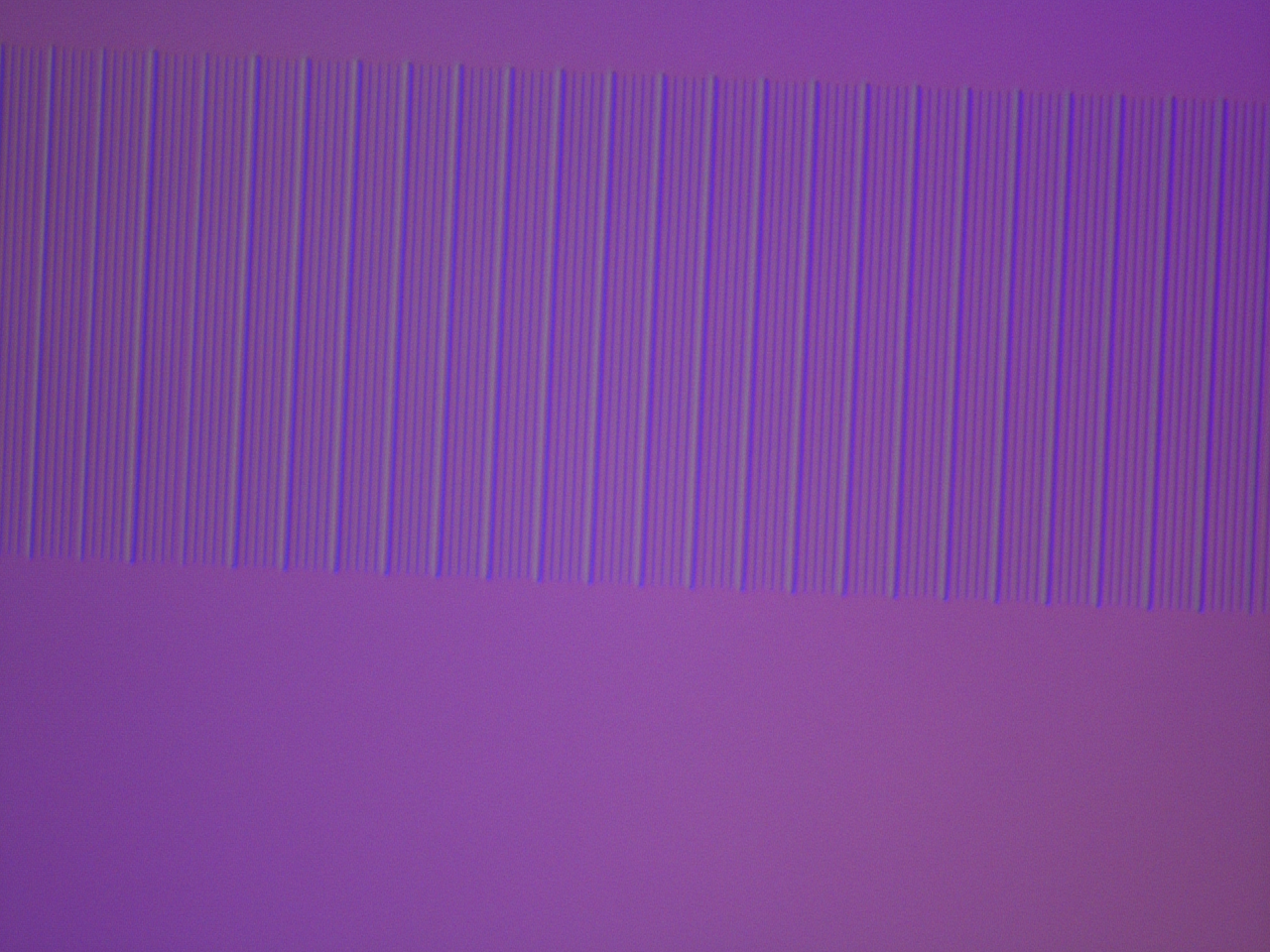
Processed wafer showing light interference
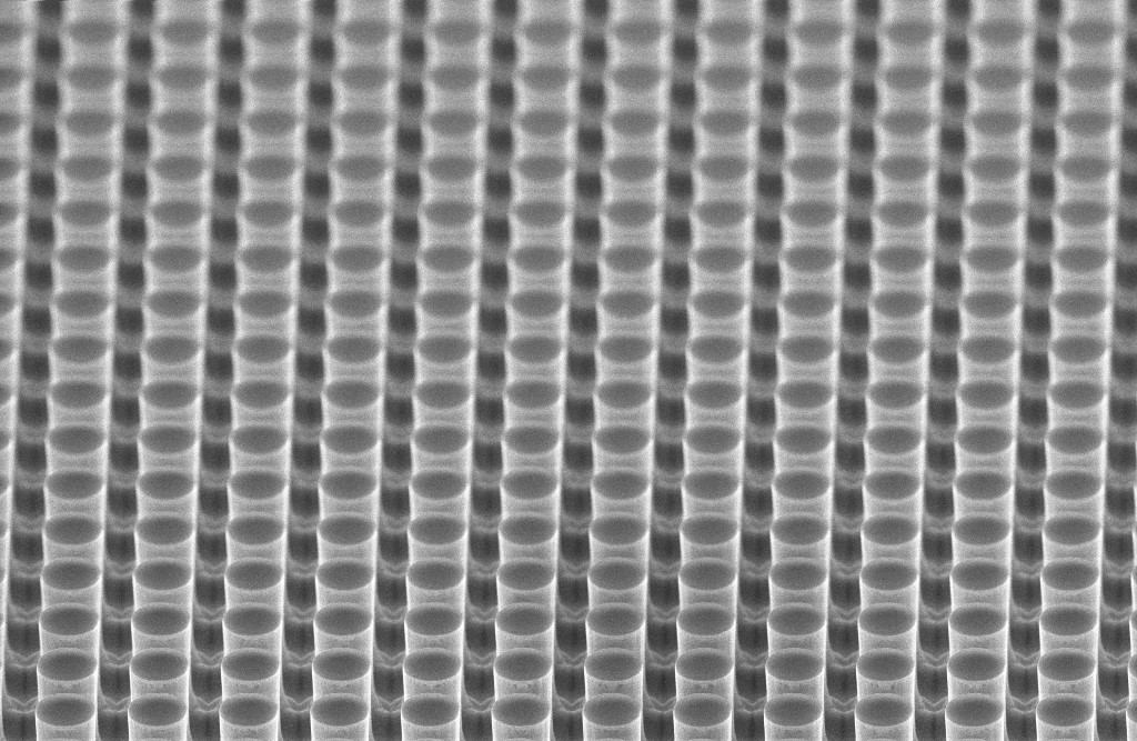
SEM image of the photonic crystal device after ICP dry-etching
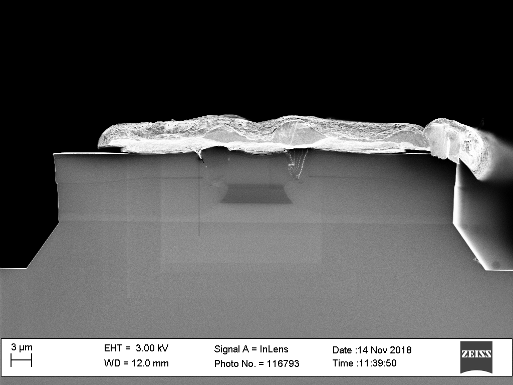
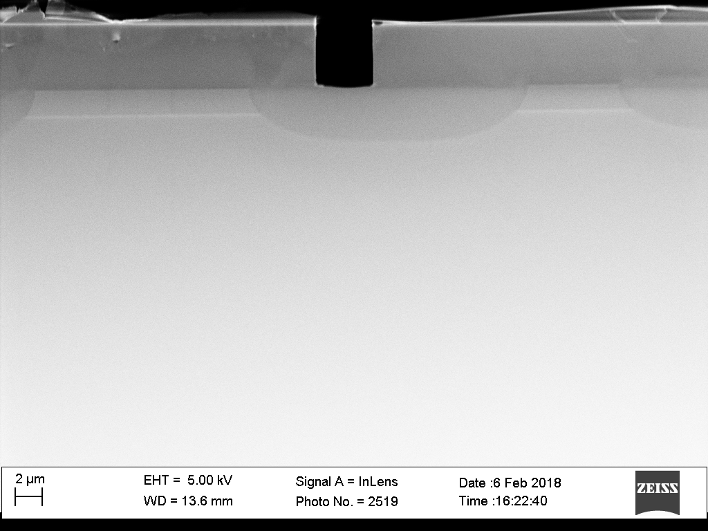
SEM picture of the cross section of a processed device
Optical picture of a grating used for a DFB laser
SEM picture of the cross section of our Vernier device
A SEM image from a Complementary Split Ring Resonator processed by Electron Beam Lithography. The resonators have different gap sizes of 2 um and 250nm.
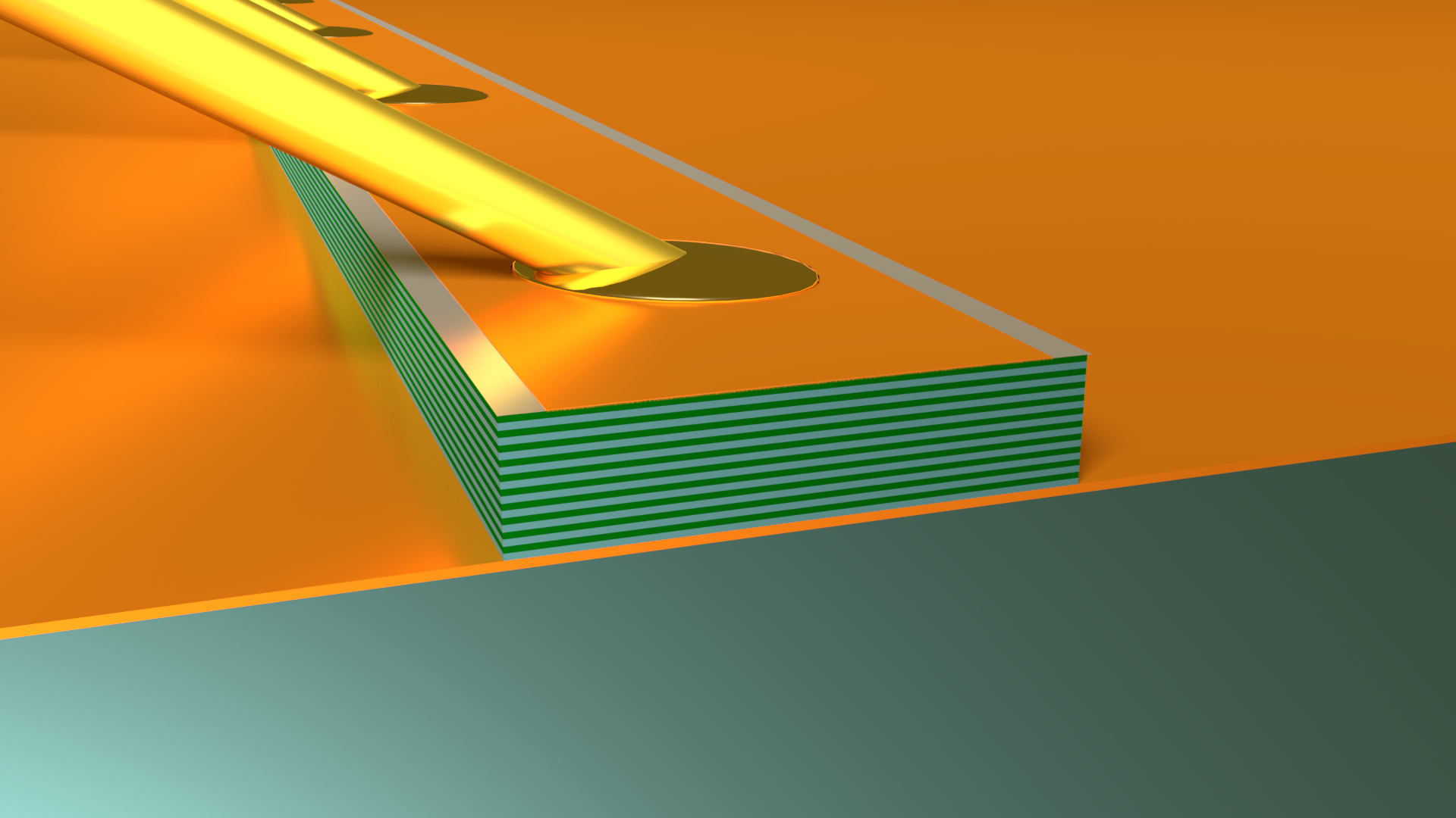
3D illustration of a double metal waveguide THz quantum cascade laser. The active region is sandwiched between two metallic plates, with wires bonded on the top metal.
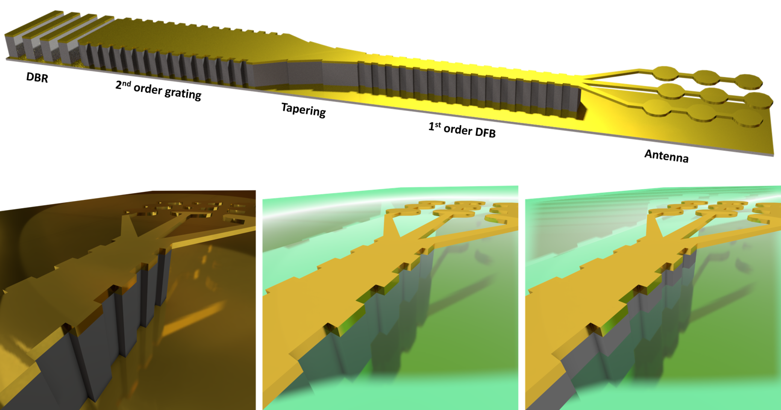
3D model of a processed Rocket Laser, showing the full device, etched front DFB (for clarity, no surrounding polymer), planarized BCB (in green; ideal case) and over-etched BCB (realistic case).
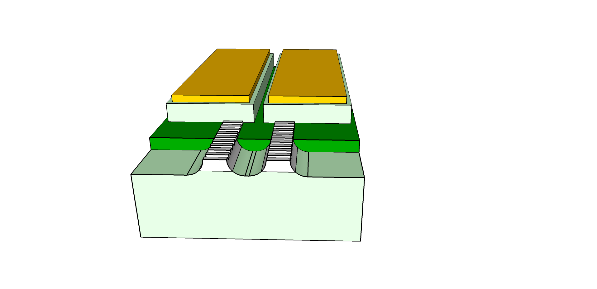
Illustration of two neighbour DFB lasers